Topic 2—Computer organization (6 hours)
2.1 Computer organization (6 hours)
--- Computer architecture ---
2.1.1
Outline the architecture of the central processing unit (CPU) and the functions of the arithmetic logic unit (ALU) and the control unit (CU) and the registers within the CPU.
Teaching Note:
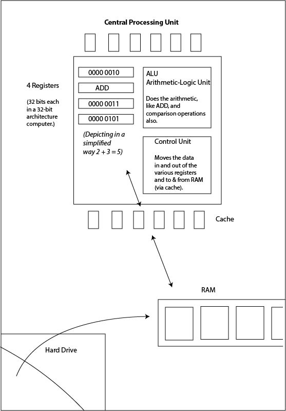
Students should be able to reproduce a block diagram showing the relationship between the elements of the CPU, input and output and storage. The memory address register (MAR) and memory data register (MDR) are the only ones that need to be included.
Sample Question - FORMER CURRICULUM:
Draw and label a basic diagram of a CPU. [4 marks]
JSR Notes -
First of all here's the Suzi inspired "Wonderful Kitchen analogy" - recall our field trip (or imagine one) to the school cafeteria to look at the kitchen, and keep it in mind when picturing this analogy.
A CPU is like a kitchen in many ways. Things are brought into it, processed in some way, and a product/products are produced.
- The arithmetic logic unit is the cutting board or the mixing bowl, where the most basic operations of cutting and mixing are done.
- The control unit is the chief chef, who keeps his eye on all the other minion chefs and instructs them what to take from where, and where to put it.
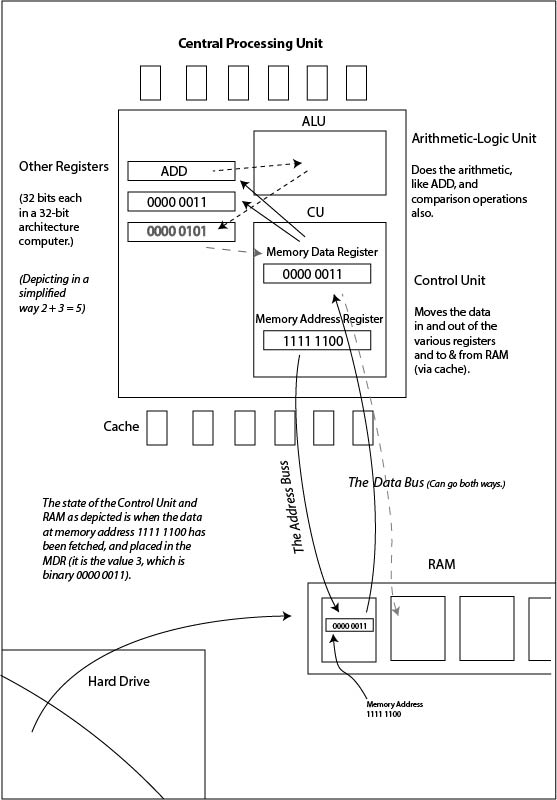
- The address bus and data bus are the various paths the minion chefs regularly tread back and forth with various stuff.
- The registers in general are various places where food in the process of being made is put.
- The memory address register and memory data registers hold the "addresses" of where those various foods should be gotten from, or go to.
- The (hard drive) storage would be the wholesale warehouse, like Macro, where the food initially comes from.
- The RAM would be the storage area in the corner, and the refrigerators.
- The cache would be where various tools and commonly used ingredients go, such as the knives holder and the salt and pepper.
See 2:45 on of the 2015 ISP video for the inspiration of this analogy.
CPU Diagram - Basic
CPU Diagram - Advanced
The summary diagram of an advanced description of a CPU is below. In terms of a quite brief summary of the full video description below.... hmmm... it would go something like this:
- data is loaded from the hard drive into the RAM
- the control unit (CU) requests a data to be fetched from a specific place in RAM
- this request, initiated with an address stored in the control unit's memory address register, goes via the address bus
- the data from that address in RAM goes back via the data bus to reside in the memory data register of the control unit
- then, basically, the control unit sends things around to various other registers to be processed eventually by the arithmetic logic unit (ALU)
Minecraft Redstone CPU Example
With the Restone mod pack for Minecraft, you can actually make your own CPU that works identically to the real thing. There are lots of full Redstone videos on YouTube that will blow you away, but at this link you'll find a good one, which has just enough detail to show you addition and subtraction.
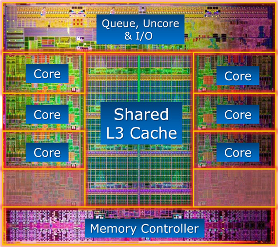
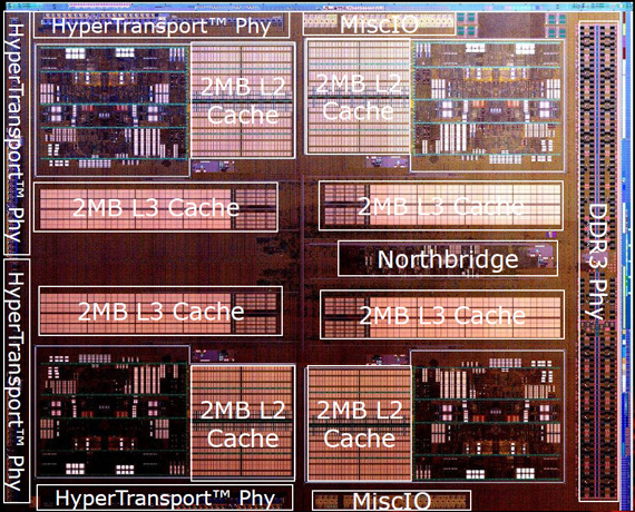
And a Couple of CPU Images: - Intel first, AMD second
------------->>>>>>>> NOTE THAT THERE IS NO NEED TO GO ANY FURTHER; WHAT FOLLOWS IS BY WAY OF ADDITIONAL INFORMATION ONLY <<<<<<------------------
JSR Notes - FORMER CURRICULUM -3.2.1 Outline the structure of the central processing unit (CPU) including the functions of the control unit (CU), the arithmetic and logic unit (ALU), primary memory and address buses.
---- From this point on, use the following legend for the FORMER CURRICULUM notes:
---- italics - the former curriculum assessment statements and teaching notes themselves
---- black, normal text - applies perfectly to this new assessment statement
---- green - pretty good fit; definitely look over and understand this
---- amber - applies, but not directly; will help your overall understanding of the assessment statement
---- gray - does not apply, but is left here to put the former curriculum notes into fuller context
First, from the teaching notes, do note that - uncharacteristically for this syllabus - you are expected to reproduce an actual diagram. And remember that the diagram in the textbook is not quite correct in that the ALU and the Control Unit are the parts that are within the CPU itself, not all the other things under the "Primary Memory" section. Though note that often times there is some cache in the CPU itself - this is called Level 1 cache. Meantime most cache of it is not built into the CPU, yet is close by - this is called Level 2 cache.
You can find lots of other CUP Diagrams on the Internet, and though they vary hugely in composition and detail, they all do have in common the two main parts: control unit and arithmetic logic unit.
In terms of the teaching note about knowing that each memory address is unique, the idea is that this must be the case, or data would get confused. And in a 32 bit system, since the registers that hold the addresses are 32 bits, the number of unique addresses that can be generated is 2 ^ 32, or around 4 billion. This is why in 32 bit systems, more than 4 GB of RAM memory cannot be addressed. In 64 bit computers - common today - the limit is 64 ^ 2 unique addresses, i.e. 16 billion billion!
JSR Notes - FORMER CURRICULUM Cont. - 3.2.3 Outline the meaning of the terms word, register and address and their
use in the storage of data and instructions.
Be sure you've got the difference between "word" and "register" straight. A register is a physical memory location with the CPU; so the smallest of the bigger cousins: cache, RAM and hard drives etc. Word is the term used to identify the amount of memory able to be passed around and worked with in a system. So we're talking a physical thing verses an amount of memory.
And, yes, the size of a computer's registers most often equates to its word size.
The teacher notes say that the study of specific registers is not required, but as you can probably imagine, there are various registers in the CPU that specialize in various parts of processing, such as address registers, data registers, conditional registers, and floating point registers, which help with real numbers. And as you would expect, the number of registers a CPU uses is most often is a significant binary number such as 32, 64, or 128, since the registers themselves will have addresses mad of a certain amount of bits.
Register and word size in most computers today are still 32 bits, but increasingly processors are 64 bit processors (with 64 bit registers, and the corresponding word size of 64 bits).
JSR Notes - FORMER CURRICULUM *** AND FROM THE ADVANCED, TOPIC 6. Added here just for those wanting a bit more information.
From 6.1.1 Describe the function of the following processor components: accumulator, instruction register and program counter.
Take a good look at the additional notes linked from this topic - they will put all of 6.1 into a bit better full context.
Remember here that the one crucial register missing is the Memory Address Register - the textbook does a good job of covering it. And do note that these are not all of the registers. Refer back to my Topic 3 notes where the CPU is discussed to get an idea of other registers. A certain processor might have 64 or 128 or 256 different registers, but these are the main ones to get your head around. So here's a summary of what each of the three registers mentioned in the syllabus do:
Accumulator - This is the register that keeps the "running total" as it were of calculations and processes. Another way to put it is that it maintains the value that is being changed on the way to a final result. For example, think of a very complex mathematical calculation; there are many "sub-totals", as it were, that need to be calculated on the way to coming up the final answer. In fact all processes executed in a computer are broken down, ultimately, to simple addition, subtraction or comparison. As these minor parts of a bigger calculation/process are processed, the accumulator keeps track of the "sub-result" that is required to be worked on next. This happens up to the point where the full calculation/process is finished, and so the final accumulated product, sitting in the accumulator, is passed back to be stored in RAM memory.
Instruction Register - This register holds the actual instructions sent from the RAM, one at a time. It is this instruction which is actually executed in the fetch and execute cycle. See the text for more good information on this, but remember that what sits in the instruction register is both an instruction, and data that the instruction will act upon (in combination with what is in the accumulator). When you think of basic arithmetic, you have an operator, like a + sign, and you have two operands, like 4, and 12. So you can think of the opcode part of the instruction as the operator, and the data part of the instruction as one of the operands; the other operand is sitting in the accumulator.
Program Counter - This just holds the address of the next instruction to be executed. As soon as the request for the next instruction is made (using the address held in the program counter), the program counter is incremented by one, so that it's ready to be used to access the next instruction in the program. You can think of the addresses as being in hexadecimal - they will actually be transferred via the address bus as 32 binary digits, or for newer computers possibly 64 binary digits. So the program counter would increment, for example ABC123 to be ABC124, to ABC125 and so on as the program executes machine code line by machine code line.